artificialintelligence
AIを活用した半導体の放射線耐性解析の加速

BitCap
AIを活用した半導体の放射線耐性解析の加速
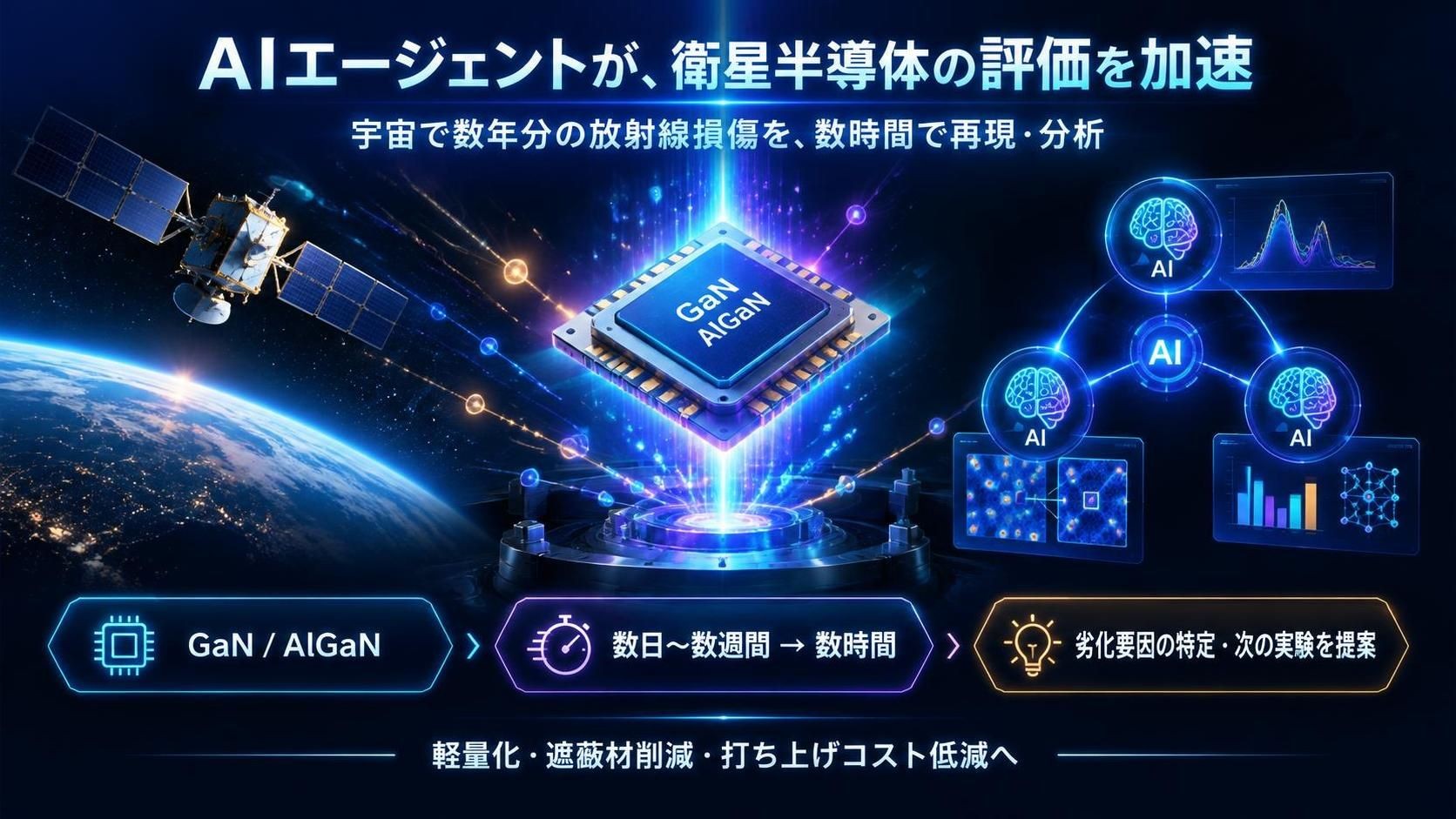
パシフィック・ノースウェスト国立研究所(PNNL)の研究チームは、人工知能(AI)エージェントを導入することで、宇宙用途向け窒化ガリウム(GaN)半導体の試験プロセスを劇的に高速化しています。この自動化システムは、イオンビームを用いて宇宙空間で長年にわたって蓄積される放射線損傷をわずか数時間でシミュレートし、データ解析にかかる期間を数週間から数時間へと大幅に短縮します。
連携して機能するこれらのAIツールは、構造的な劣化箇所を特定するだけでなく、次の試験パラメータを提案することで、研究ワークフロー全体を効率化します。
衛星の重要な構成部品であるこれらの半導体の放射線耐性を向上させることで、重い遮蔽(シールド)が不要となり、結果として製造コストや打ち上げコストの削減につながります。
この技術的飛躍は、過酷な環境下で使用される高度なマイクロチップを製造する企業に注目する投資家にとって、大きなビジネスチャンスをもたらす可能性があります。
AIエージェントの活用により、長年にわたる放射線損傷をわずか数時間で解析可能に。衛星向けGaNチップの開発が加速しています。
米国のパシフィック・ノースウェスト国立研究所(PNNL)は、AIエージェントを用いて半導体の放射線損傷を解析しています。
初期成果:
- 衛星やレーダーシステムなどに使用されるGaN(窒化ガリウム)およびAlGaN(窒化アルミニウムガリウム)チップの試験。
- イオンビーム照射により、宇宙空間で長年かけて蓄積される損傷をわずか数時間で再現。
- 従来は数日から数週間を要していた実験データの解析を、わずか数時間で完了。
- 複数のAIエージェントが連携し、劣化メカニズムの特定や新たな実験の提案を行う。
衛星は、放射線にさらされる環境下で10〜15年間にわたり稼働し続ける必要があり、メンテナンスを行うことは不可能です。
チップ自体の耐性を向上させることで、遮蔽材の削減、軽量化、そして打ち上げコストの低減が可能になります。
投資家の視点からは、WINセミコンダクター(WIN Semiconductors、証券コード:3105)のような、III-V族半導体を製造する企業が注目されます。
AIはチップの設計だけでなく、過酷な環境下での使用に向けた認定(クオリフィケーション)プロセスをも加速させる可能性があります。
アジア半導体市場の主要指標
Accelerating Semiconductor Radiation Analysis with AI
Researchers at the Pacific Northwest National Laboratory are dramatically speeding up the testing of gallium nitride semiconductors intended for space applications by deploying artificial intelligence agents. By simulating years of orbital radiation damage in mere hours using ion beams, the automated system drastically cuts down data analysis timelines from weeks to hours.
These collaborative AI tools not only pinpoint structural degradation but also suggest subsequent testing parameters to streamline the overall research workflow.
Enhancing the natural radiation tolerance of these vital satellite components allows engineers to eliminate heavy shielding, which ultimately lowers overall manufacturing and launch expenditures.
Consequently, this technological leap creates lucrative opportunities for specialized investors monitoring advanced microchip producers suited for harsh environments.
Years of radiation damage analyzed in just a few hours thanks to AI agents. Development of GaN chips for satellites is accelerating
The U.S. laboratory PNNL is now using AI agents to analyze radiation damage to semiconductors.
Initial results:
-Tests on GaN and AlGaN chips, used notably in satellites and radar systems.
-Ion beam irradiation to reproduce, in just a few hours, damage accumulated over years in space.
-Analysis of experimental data in just a few hours, compared with several days or weeks previously.
-Multiple AI agents collaborate to identify degradation mechanisms and propose new experiments.
Satellites must operate for 10 to 15 years despite radiation exposure, with no possibility of maintenance.
Improving chips’ inherent resistance would make it possible to reduce shielding, weight, and launch costs.
For investors, III-V semiconductor manufacturers such as WIN Semi (3105) are worth watching.
AI could accelerate not only chip design, but also their qualification for extreme environments.